

Researchers Develop Hydroprinting Method to Print Conductive Patterns onto 3D Structures
At the end of 2015, The Hebrew University of Jerusalem announced the opening of a new 3D and Functional Printing Center. The director of the center is Professor Shlomo Magdassi, whose innovative research was responsible for the production of the conductive nano-inks used by Israeli 3D printed electronics company Nano Dimension for its flagship DragonFly 2020 circuit board 3D printer, which continues to be delivered to beta customers all over the world. Professor Magdassi and The Hebrew University of Jerusalem are back in the 3D printing spotlight again with some more cutting-edge research about printed electronics.
 A lot of focus has been placed in recent years on producing 3D structures with conductive features, particularly in terms of the Internet of Things. The difficulty that arises when attempting to print conductive structures onto 3D objects comes from the sometimes uneven and complex topography of substrates, which makes it difficult to deposit liquids onto the surface. The substrate must be facing the nozzle for the material to be deposited, and only one material can be printed at a time, which is obviously time-consuming, and at times can end up with unevenly spread ink, making the devices non-reproducible.
Professor Magdassi, together with other researchers from The Hebrew University of Jerusalem and the Nanyang Technological University in Singapore, recently published a paper in Advanced Materials Technologies, titled “Hydroprinting Conductive Patterns onto 3D Structures.” The paper presents their method of using a hydroprinting process to fabricate conductive circuits and patterns. Co-authors included Professor Magdassi, Gabriel Saada, and Avi Chernevousky with The Hebrew University of Jerusalem and Dr. Michael Layani with Nanyang Technological University.
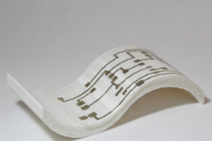
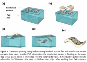 Hydroprinting is often used to print graphic designs onto uneven surfaces, mostly for the automobile and decorative industries. This technology can get around the difficulties of the transfer methods mentioned previously by printing a whole pattern onto a 3D object, from all facets, in just one step. No polymer layers are involved in the process, so conductive materials can be deposited directly on top of each other.
This new strategy is expected to benefit multiple applications, including soft robotics, biomedical devices, 3D electronics, and 3D printed antennas used for communications.
Professor Magdassi told 3DPrint.com, “The method is expected to lead to important applications in the fields of biomedical devices and Internet of Things (IoT). As a proof-of-concept, it was already implemented by hydroprinting Near Field Communication (NFC) antennas on curved surfaces such as bottles and 3D printed objects. This was presented in the recent LOPE-C conference competition, under the ‘ReadSpot’ project.”
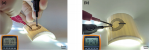 According to the paper’s abstract, “A novel and facile method for printing functional conductive patterns on 3D objects with unconventional angles using hydroprinting of silver nano-particles (NPs) ink is developed. Silver NPs ink is inkjet printed on water soluble polyvinyl alcohol films. Sintering at room temperature is achieved by exposing the printed pattern to hydrochloric acid fumes. Electric circuits are hydroprinted at low temperature (50 °C) on various 3D-printed structures and materials. The conductive patterns are hydroprinted on hard 90° angle objects and are assembled without any presence of sacrificial layer, which allows layer-by-layer overlap hydroprinting. In addition, electric Light Emmiting Diode (LED) circuits and heater are successfully hydroprinted. To show the applicability of the process we hydroprinted a fully functional Near Field Communication (NFC) antenna onto a curved object, which was successfully paired with a smartphone. Analysis of hydroprinted patterns shows that the resistivity is 17.1 times higher than silver bulk which is considered suitable in most application.”
This breakthrough method only takes minutes, and experiments are currently being conducted to hydroprint whole optoelectronic 3D devices. In addition, the research team discovered that their method would also work to fabricate multi-layer circuits, just by repeating the process as many times as there are layers.
Source: 3dprint.com


